
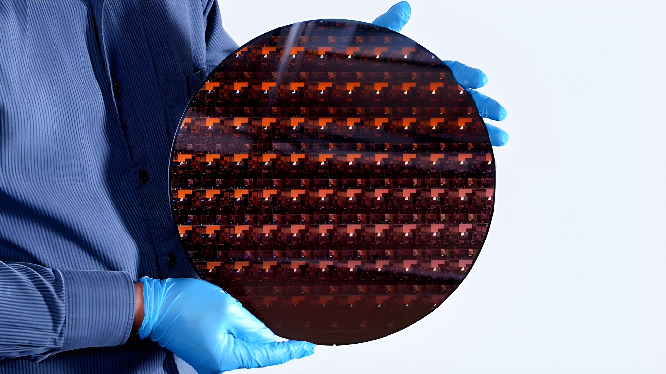
Technology corporation IBM has established a physical presence in Chitose, Hokkaido, deepening its collaboration with Japanese semiconductor foundry Rapidus as the company accelerates preparations for advanced chip manufacturing. The move serves to bolster technical transfer, workforce development, and operational readiness for Rapidus, which holds a licensing agreement for IBM’s 2-nanometer manufacturing technology and works alongside the U.S. firm in joint research and development.
Rapidus stands as a central pillar in Japan’s national strategy to revitalize domestic semiconductor capabilities. The enterprise relies on backing from the Japanese government alongside investments from prominent industrial groups including Toyota, Denso, Sony Group, SoftBank, NTT, Kioxia, NEC, and MUFG Bank. Through this broad coalition, the initiative seeks to narrow the technological gap separating Japan from global foundry leaders such as Taiwan Semiconductor Manufacturing Company, Samsung Electronics, and Intel.
Construction of the primary fabrication facility in Chitose continues to advance, with the company having successfully initiated equipment installation for its trial production line. Over the coming months, Rapidus intends to expand its process verification scale to lay the groundwork for commercial manufacturing. Japanese authorities have channeled substantial financial subsidies into the venture, viewing domestic production of advanced logic chips as a critical matter of economic resilience, national security, and supply chain independence.
Rather than adopting a traditional incremental approach of upgrading through mature nodes, Rapidus has chosen to leap directly into the 2-nanometer generation. While industry analysts regard this aggressive strategy as carrying considerable execution risk, a successful rollout would instantly position Japan back at the cutting edge of global logic chip production after decades out of the market. By pairing IBM’s foundational transistor and process innovations with Japan’s manufacturing infrastructure, the partners aim to bridge the gap between laboratory research and commercial fabrication.

Observers identify 2027 as a decisive watershed for the enterprise. Meeting the target date for mass production would reestablish Japan within the top tier of semiconductor manufacturing while offering international markets an alternative source for advanced logic chips, potentially easing heavy reliance on existing geographic production hubs.